Low Noise Amplifier
RF communication is based on four major components: the antenna, low noise amplifier (LNA), gain block, and mixer. During a design course at UTK I designed a LNA. The LNA is a specially configured circuit which aims to reduce the noise coming from the internal physics of the transistor and increase robustness to transmitted noise. Noise handling in the LNA device is done by creating a better impedance match and managing the gain requirement.
As a member of a design team, one of the designed circuits I submitted was the LNA. I began the process with simulation, using Keysight’s ADS software, for the most simplified version of the circuit. Because the LNA’s transistor operates in a stable and linear region, our simulation can take advantage of the Scattering Parameters (S-Params).
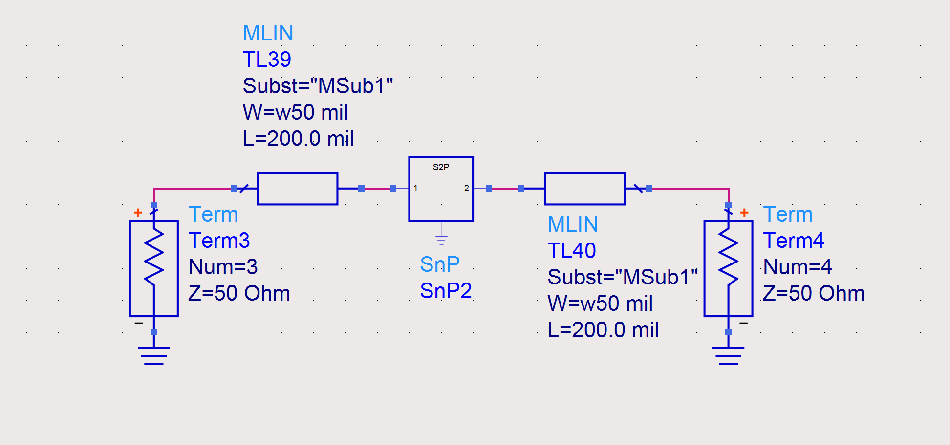
Above is a picture of the first circuit simulation. Here we are creating a matching network taking into account only the transistor. Throughout the design process our ADS model will become more accurate, and close in on a design solution to the optimization parameters.
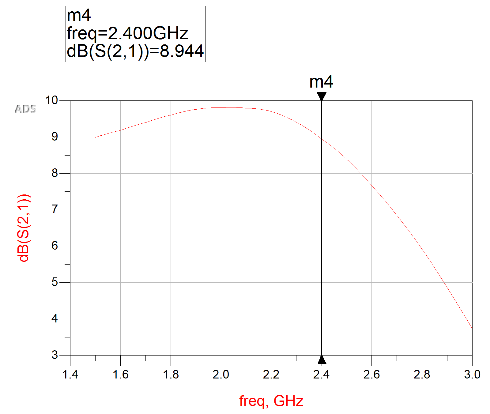
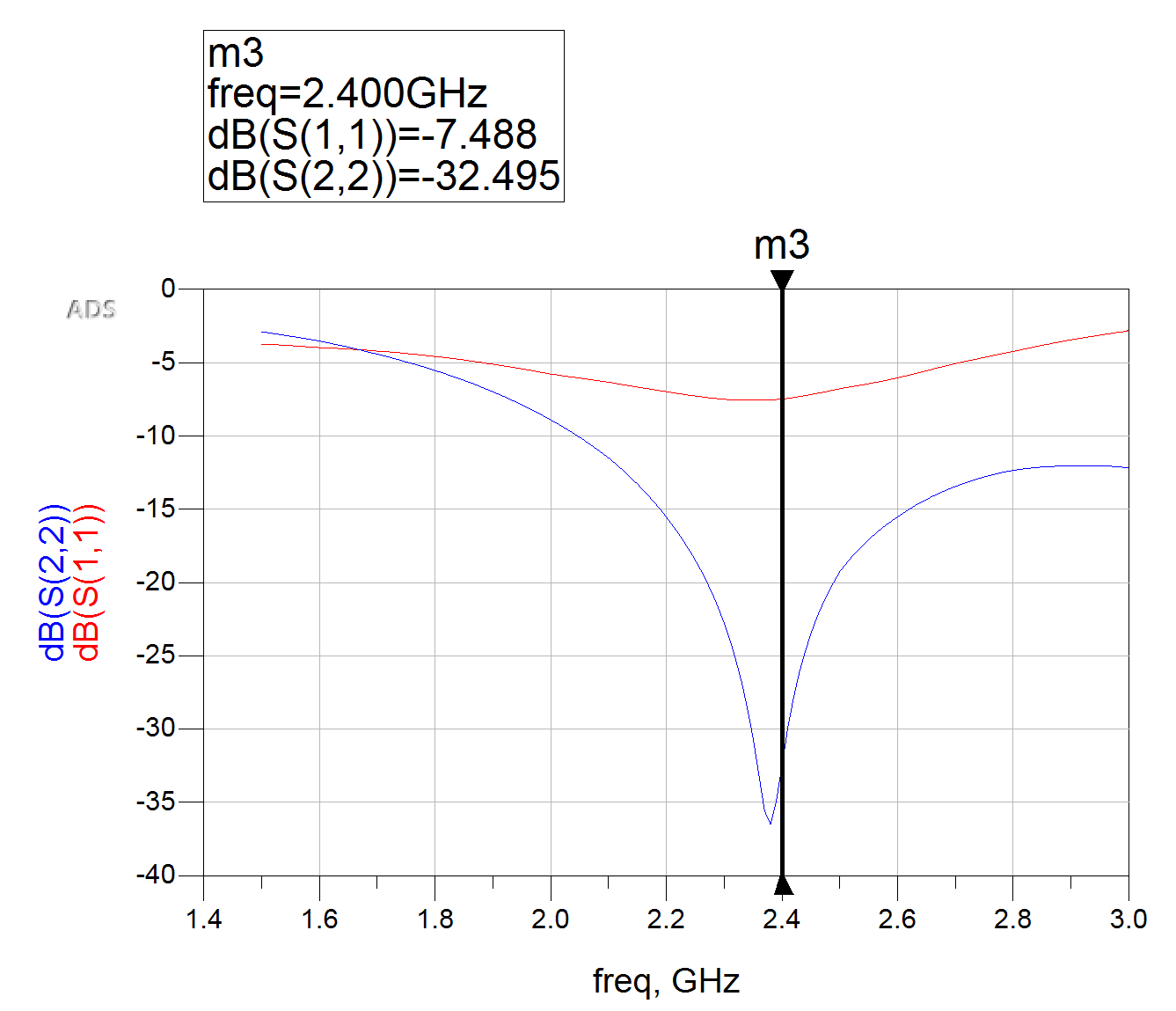
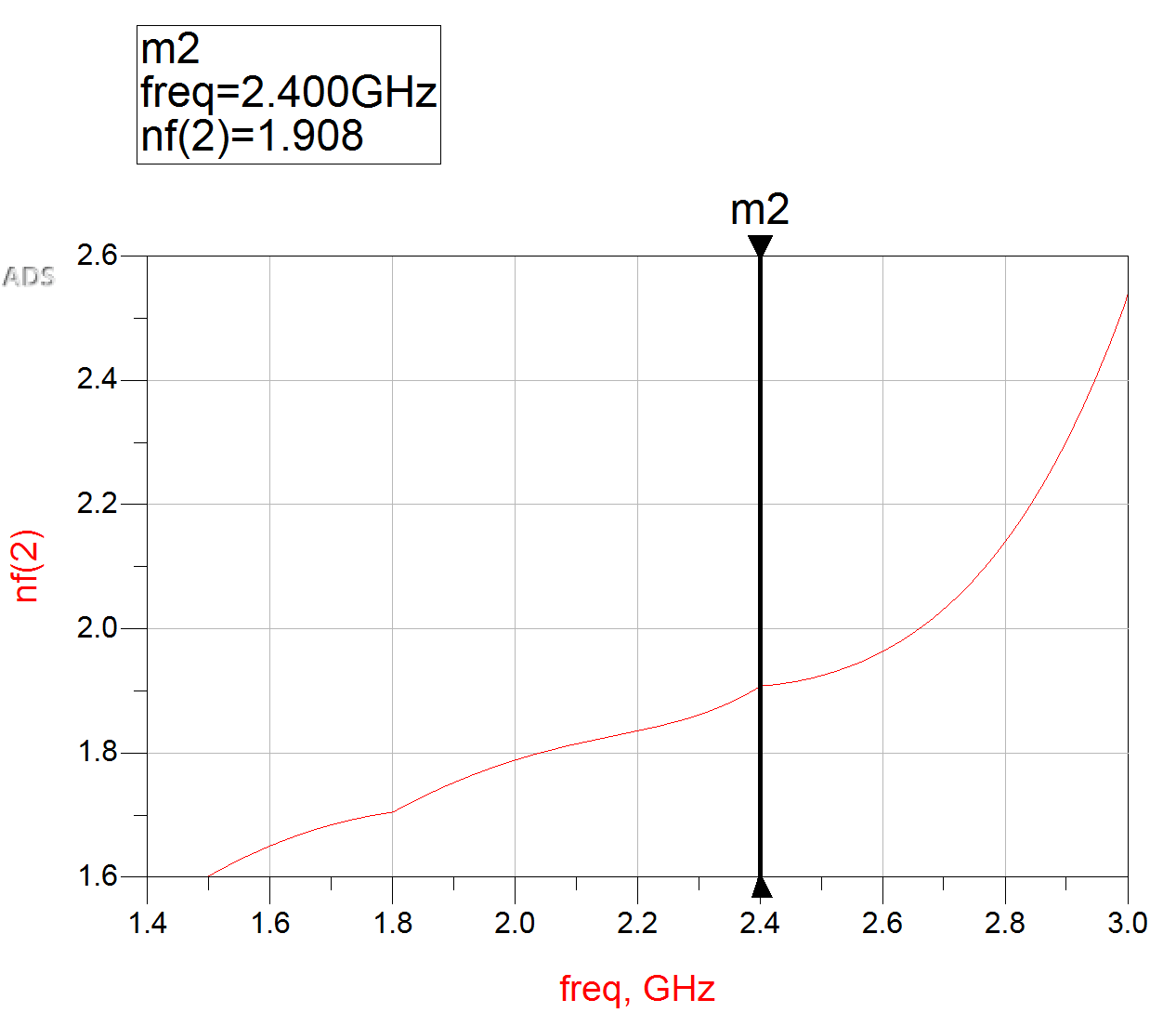
Our circuit is to be made to match these parameters:
- $S_{22} < -25$dB
- $NF(2) < 1.99$
Using these constraints we will optimize the micro-strip line dimensions to change within a $\pm5\%$ range. These goals represent the insertion loss($S_{22}$) and the simulated noise at 2.4 GHz. The noise figure value is determine from the simulated noise circle from the smith plot below.
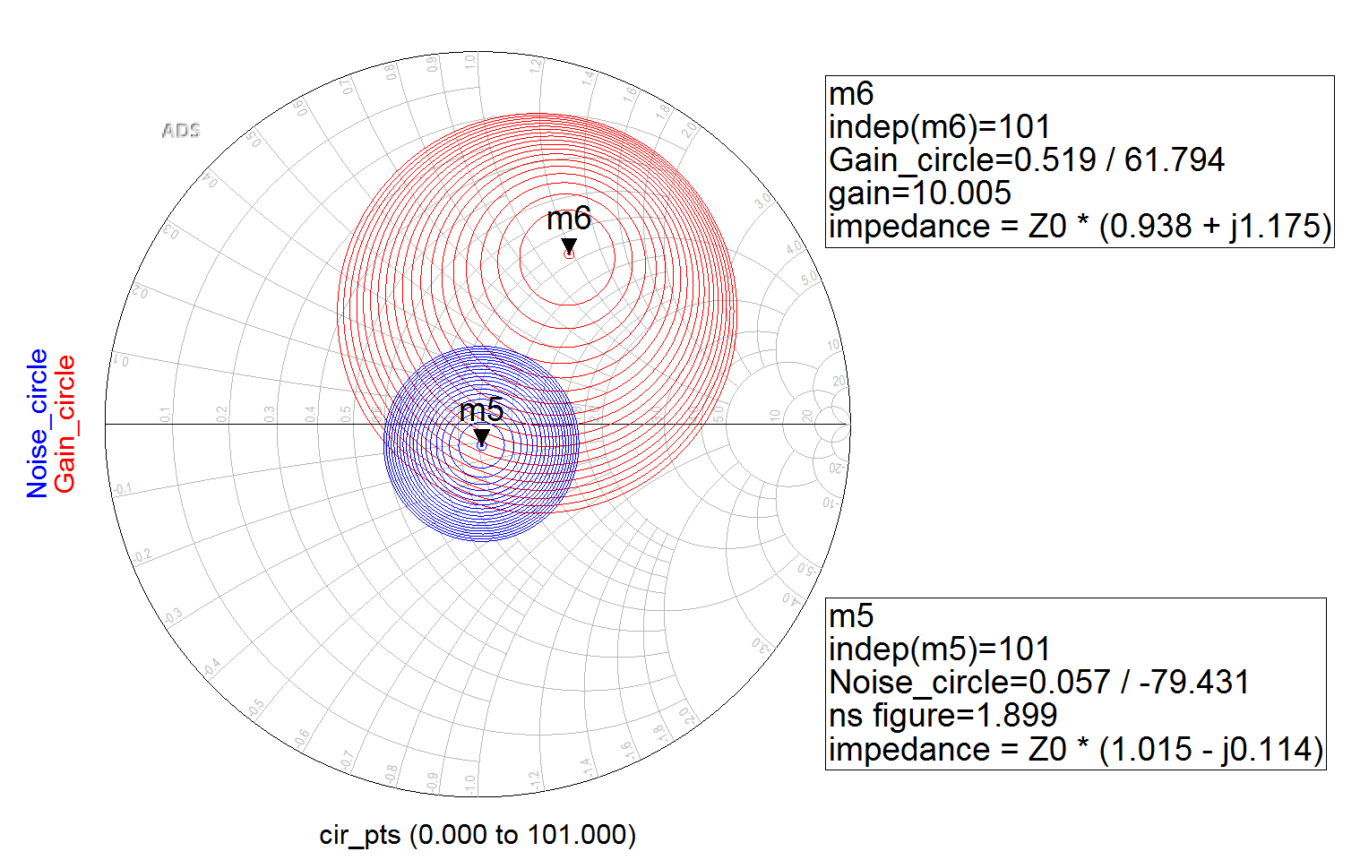
Advancing the circuit model, we used stub matching. This is done by determining the input and output impedance and creating a transmission lines with the complex conjugate of the impedance. Then with a stub matching network established, the transistor bias lines could be added to our model.
Design Specifics
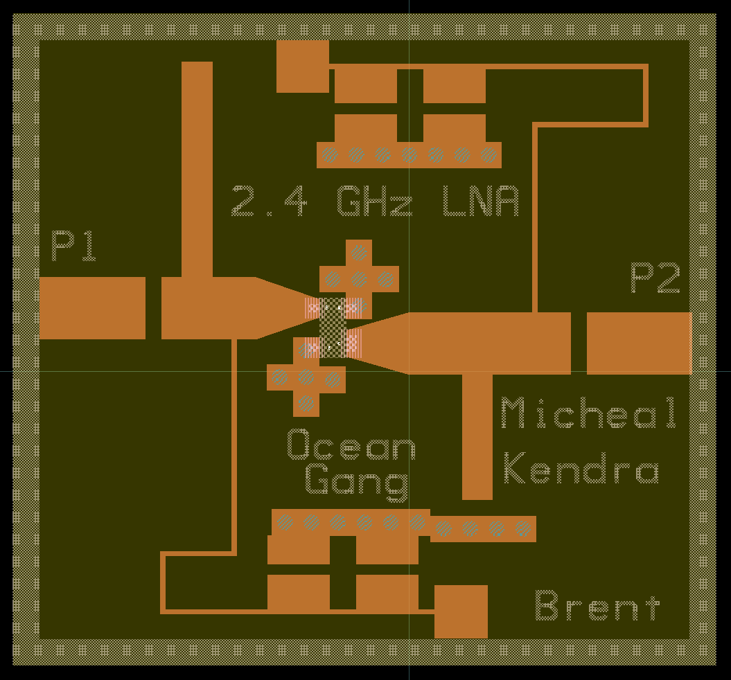
Using two capacitors at 1nF and 10nF for the bias lines, the DC source will not be able to add any AC noise to our circuit. The transistor for the LNA, was an AT-41511 BJT and the substrate for our circuit is FR4. As proper design practice approximately 5 vias to the ground plate were used to minimize the introduced inductance by the connection. The bias line width is set to 10 mils because it was the smallest line width possible for our fabrication.
LNA Results
